Semiconductor inkjet solutions
Semiconductor inkjet solutions
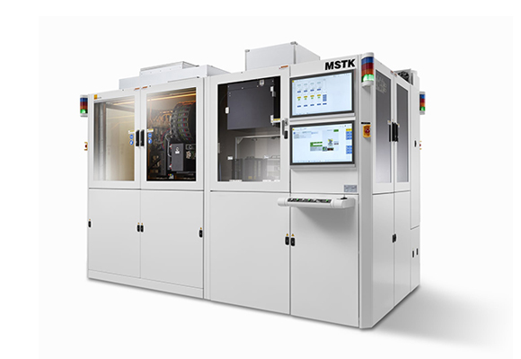
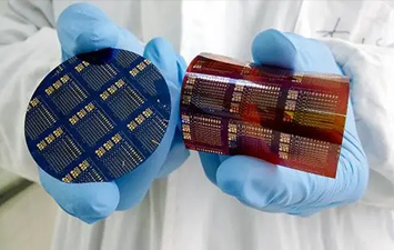
This solution provides a wide range of front-end and back-end processes for the semiconductor industry. The platform has integrated edge processing capabilities that can handle any substrate type or wafer size, and is integrated with MES systems (SECS-GEM) as well as the latest preprocessing and post-processing modules. Our nozzle replacement method and complete process control can improve yield and process stability. This system can be used in conjunction with high-precision allocation units, further expanding the window for machinable materials on the same platform。
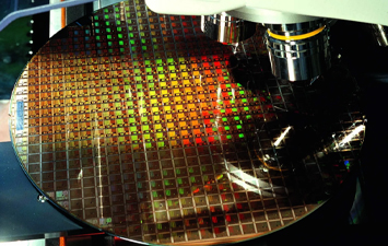
Process field
- Photoresist (photoresist) printing
- Deposition of sensor active ink
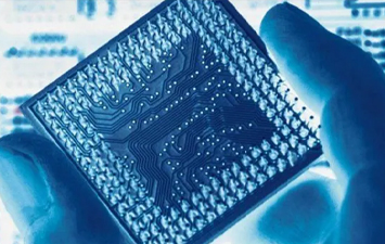
- Chip packaging
- Printing of dielectrics, conductive agents, corrosion inhibitors, and adhesives
- High precision inkjet printing
- Better landing accuracy than 5 microns
- High uniformity
- Up to 8 different liquids can be used in one printing process
- Can support industrial inkjet print heads of different brands
This system platform has solutions that can be applied to multiple applications. Our printing strategy improves platform availability and process yield by minimizing the need for manual intervention or manual mechanical calibration of nozzles. Our advanced nozzle maintenance system, which has been verified on-site, can extend the normal operation time of the platform. Not directly contacting the nozzle area can improve inkjet stability and extend the lifespan of the nozzle. Our nozzle automatic calibration and advanced nozzle replacement strategy can provide you with comprehensive process control and reliable printing results。
Automation&Process IntegrationThis platform comes with optional wafer processing functions, which can also handle substrates of different sizes, and can be equipped with more pre-treatment and post-processing stations, providing integrated solutions for your process requirements:
- Cassette The motion robotic arm includes wafer mapping and front calibration
- Plasma Cleaning, hot plate, UV curing, and others
Conversation with representatives
16th Building F2, Yuefu Avenue, Liangjiang New Area, Chongqing

© 2024 All rights reserved by Inkjet Research Institute. All rights reserved。渝ICP备2022008663号-1
