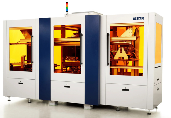
This solution replaces the subtractive process chain with the layered process steps in electronic production, which has always been one of our transformation concepts. It reduces material waste and improves production efficiency. Most importantly, this solution improves process stability and has become a new feature in today's electronic component production process. This breaks through the limits of current production technologies for rigid and flexible circuits using any substrate material. Whether it is single chip PCB panels or FPC roll to roll double-sided technology, they will be the preferred platform for the production of stacked electronics。

Process field
- Character and Variable Data Printing
- Solder mask printing
- Anti etching printing
- Printing of conductive layer, dielectric layer, and active layer
- Material deposition (layer by layer) printing
- Nano metal ink printing line for conductive electronic circuits
- Draw blue LED based on polymer
- Deposition of catalysts for carbon nanotube growth
Using our solder mask printing solution to print solder mask layers, developed specifically for industrial production, it is powerful and performs the best. It is also possible to choose a system that integrates automatic loading and unloading of substrates for printing FPC electronic products. Functional materials are applied with high precision to print antennas, sensors, or touch displays on PET films. Other application areas are medical technology or battery or fuel cell production。
优势- High precision printing - can also be printed on both sides
- High output speed
- Modular roll to roll system: network operation control for unwinding and rewinding systems
- Rolling buffer
- Pre processing, such as plasma cleaning
- Fully integrated spray printing system
- Integration of UV and post baking treatment
- Collaborating with leading automation equipment manufacturers
Based on the solution, we also provide a system that can handle UV curing and etching resistance. This system can be used for the application of different corrosion inhibitors in PCB production or micro etching. Anti etching process is a three-step digital printing process that can increase production and quality while reducing manufacturing costs. The steps are: pre-treatment, direct inkjet printing with resistance to etching, in-situ UV drying, and etching/cleaning。
advantage- X-axis and y-axis: excellent linear spatial definition
- 标准L/S 距离 < 70 µm
- Good adhesion to copper, stainless steel, brass, and other metals


