Fujifilm's Attempt on MEM
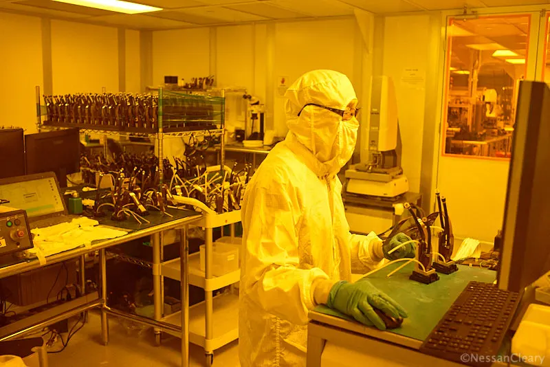
In the past few years, Fujifilm has been quietly upgrading its Dimatix manufacturing plant located in Santa Clara, California, which is home to Samba print heads. Therefore, I visited the factory to better understand the working principle of MEM manufacturing process and what it means for the final print head。

Dimatix has all manufacturing factories located in the United States. The company's main base is located in New Hampshire and serves as the headquarters for Fujifilm's print head product portfolio, including the StarFire and Sapphire series, all of which rely on high voltage electrical technology. The Santa Clara factory in the heart of Silicon Valley in the United States is a very different reconstruction. This is specifically designed for the use of microelectromechanical systems or MEM methods. Essentially, this means using semiconductor technology to build actuators, achieving higher complexity and accuracy.
And, as Bailey Smith, Executive Vice President of Business Development, pointed out, this in turn means establishing a foundation in Silicon Valley: "If you try MEM, there are only a few places that can be achieved. There are a lot of silicon MEM facilities here and Silicon Valley. You must have the expertise we have in nitrogen and chemical storage. It is impossible to recruit these people in New Hampshire. (The factory consumes a large amount of liquid nitrogen, which is used in production equipment) Create an anaerobic atmosphere to prevent copper oxidation in electronic circuits." Dimatix was founded in 1984 and decided to invest in MEM, which was still owned by Markem Corporation at the time. In order to ensure the smooth progress of the matter, the company purchased some silicon wafer factory equipment, which had a history of 10 years at that time.
Meanwhile, Fujifilm realizes that digital printing will eventually replace offset printing and hopes that digital printing can replace its CtP business. Therefore, Fujifilm has begun the development of JetPress digital printing machines. The company ultimately acquired Sericol, which developed UV ink, in 2005, Avecia, which specializes in producing water-based ink, and Dimatix in 2006. Smith pointed out that the core of Fujifilm is a technology company. They hope to have the technology to produce their own products.
He continued, "They know JetPress needs high-quality printing, and they have already started researching MEM in Japan. But when they see what we are doing, they are very interested."。

Fujifilm Dimatix has established a dedicated MEM manufacturing factory in Santa Clara。
Dimatix's initial efforts in MEM were based on bulk piezoelectric technology. But Fujifilm has developed a different method, namely sputtering PZT, which has proven to be more effective and has been adopted by Dimatix. Smith explained, "Fujifilm in Japan has a core patent. They authorized us with this technology, and we modified it to make it productive. We customized the tools, which was a challenging task.".
It should be pointed out that sputtering PZT is one of the several methods that can be used for MEM to manufacture print heads. It is different from the methods used by other print head manufacturers such as SolGel. Smith said that sputtering PZT is more durable and can make magnetic heads more suitable for industrial production, but of course, other manufacturers also say the same thing about their magnetic heads!
Most piezoelectric printheads use piezoelectric lead titanate (commonly referred to as PZT) because of its highly efficient piezoelectric properties, which change shape when applied with pressure. The piezoelectric printhead utilizes this shape conversion to transfer ink from the ink chamber through the nozzle.
Fujifilm's method involves using RF magnetron sputtering to form a PZT thin film layer on a silicon substrate, producing a piezoelectric coefficient of d 31=-250pm/V, which is said to be about 70% higher than traditional techniques. This may be fatal due to the use of approximately 13% concentration dopants and very precise control of crystal arrangement, which is crucial for controlling the distortion mode of PZT.
Smith stated that the main advantage of this method compared to other technologies introduced, including SolGel, is the biggest advantage of PZT: "The sputtering process we created is practical. For bulk piezoelectric, they place and form bulk crystals, which then have to be uniformly scanned at very high temperatures, which is a considerable challenge. When we deposit PZT, it has already been scanned, so there is no need for high temperatures to be processed, which means we do something about the MEM structure.".
He continued, "One of the loose standards we have is our deviation from fixed wavelengths, which we are among the top in the world. If we apply too high a temperature, we can take them to extremes. We believe we have the best PZT, and many other companies come to us to use our products.".
He added, "We have a small group of people engaged in the research and development of other potential applications of MEM using sputtered PZT, which is why our company is famous for this type of work. We will be developing some of the products we produce in New Hampshire here. They will only be used for engineering and development, not production. We are still working in the targeted field and some medical equipment fields, but not our main area. A larger width."
Microelectromechanical systems combine electronic devices with mobile components, allowing complex designs to be executed in very small spaces. The material selection for building these systems is limited, with silicon being the most common material so far due to its long service life and easy integration of electronic functions. Therefore, Si MEM can be constructed using a process similar to manufacturing semiconductor devices. Therefore, a deposition layer material, such as silicon with PZT thin films, can be used to create patterns within these layers using photolithography, thereby creating channels for electronic circuits and fluid management.
Each Samba print head has an EPROM module that contains information about its performance。
This process starts with lithography. Smith explained, "This is a semiconductor process. Therefore, we have to go through a multi-layered construction process. We may have 20 layers, and each function is added to these different layers. Therefore, we add one function at a time. Then we install it and perform metalization functions. These functions include separate layers for recirculation fluid management.".
This work was completed using the ASML stepper provided by the Netherlands.
Smith added that Dimatix is using a more professional variant: "This photo tool is because we have patterns in layers for thousands of years, so we have to align the front features with the back features. This results in specialized processing where we cannot run the wafer on the tool, which can scratch the bottom of the wafer. Therefore, because we protect both sides of the wafer, the ASML stepper is very reliable.".
Darren Imai, Vice President of MEM R&D at Fujifilm Dimatix, pointed out that "these are very precise structures, ranging from around 400 to 650 microns, sometimes as small as 10 microns, so handling this geometric shape can be a very professional job.".
In the past few years, Fujifilm has modified some wafer factory tools to produce larger wafers, increasing from 6 inches to 8 inches. The chips that make up the foundation of Samba print heads are directly cut from these wafers, so the direct benefit of larger wafer sizes is the improvement of manufacturing capabilities. A 6-inch wafer can produce 10 chips, but an 8-inch wafer can produce up to 21 chips.
In addition to additional capacity, device upgrades have also produced better results, as Imai explained: "We can achieve uniformity of 8-inch PZT more effectively than 6-inch. He stated that switching to larger wafers requires a lot of funding and simulation work, and pointed out:" We have improved consistency across the entire platform. Because we have upgraded many devices, some of which are already 30 years old. We have adopted more advanced new equipment, which brings us more process advantages. ".
But one of the challenges in transitioning to larger wafer sizes is to continue manufacturing in the factory while upgrading the machines, which also aims to limit the size to 8 inches. Fujifilm can upgrade its existing tools to handle 8-inch wafers, and if dealing with larger flexible sizes, it must start from scratch.
These molds form the foundation of Samba print heads, including electronic devices and fluid channels. However, this is not the whole story, as many other components must also be added. This includes the nozzle plate at the front end of the mold. There are ink channels and electronic connections inside.
Another important component is the mounting bracket, which allows the pan tilt to be correctly installed and calibrated with minimal hassle. There is also an EPROM module that includes parameters such as voltage coefficient, testing, and magnetic head level. It will take approximately three months to produce one Samba printhead in total。
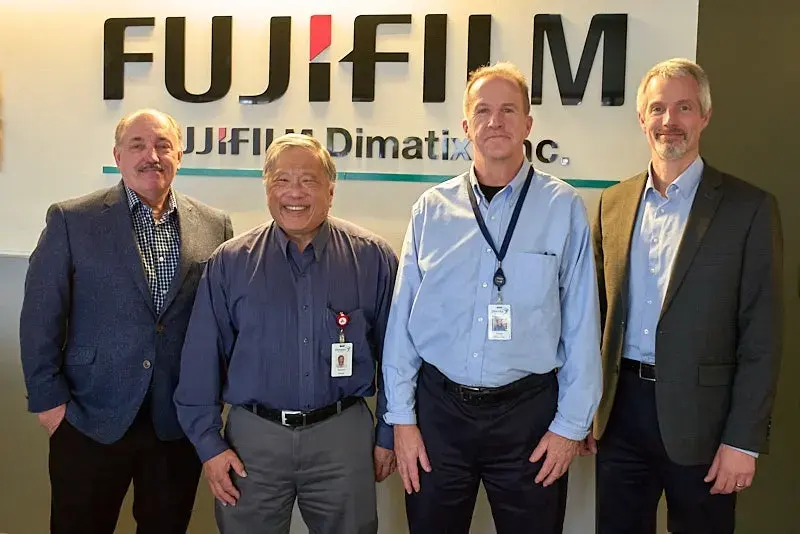
From left: Dave Pulizzi, Vice President of Operations; Darren Imai, Vice President of MEMS Research and Development; Terry O'Keefe, Senior Product Manager; Bailey Smith, Executive Vice President of Business Development. Terry O'Keefe, Senior Product Manager of Samba Print Head, stated that MEMS manufacturing is an inherent component of Samba's feature set, and pointed out that "as ink droplets become smaller and all the problems caused by turbulence, we want to have all these detailed tasks close together. The faster you run, the more everything becomes. Being able to integrate all these important functions into a small space is one of the characteristics of MEM.".
O'Keeffe stated that the material group must be chemically compatible with most of the fluids used by the customer, and pointed out that "we complete all the work internally. The entire process from design to testing. We have jet aircraft design experts. This is a process through which we can test and obtain some information, and all of this is done internally.".
Smith explained, "We invest a lot of energy in material testing. We hope to predict the use of jet aircraft. Generating pistons requires a lot of energy, but it can generate some feedback and crosstalk between nozzles. We have developed many production tools that are better than any other product on the market.".
In short, the Dimatix factory located in Santa Clara is very impressive. It is almost entirely dedicated to building Samba print heads. The entire factory operates extremely (24/7) with approximately 300 employees. Pipelines and cables are arranged on the ceiling, and each individual process has a dedicated room, including a dedicated clean area. The recent updates ensure that Dimatix has sufficient production capacity to meet demand before 2027. Dave Pulizzi, Vice President of Operations at Clara Factory, said, "We have developed a plan to exceed this goal when necessary.".
There is more to this story, and I will gain a more detailed understanding of Samba print heads, as well as how they benefit from Fujifilm's decision to implement MEM methods for you, and how to convert them into the current single channel tray printer。
Conversation with representatives
16th Building F2, Yuefu Avenue, Liangjiang New Area, Chongqing

© 2024 All rights reserved by Inkjet Research Institute. All rights reserved。渝ICP备2022008663号-1
